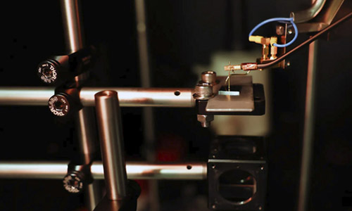
Imec sets up R&D activities in Hokkaido, to boost Japan’s photonics chip sector…
…and Hamamatsu Photonics opens new production facility in Switzerland.
17 November 2026
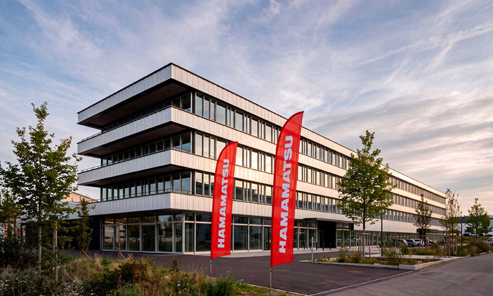
HamamatsuSwitzerland’s new facility offers more than 3,000 m2 of space, including 1,350 m2 of cleanroom facilities. Photo: Hamamatsu.
Imec, a a global center for advanced semiconductor research and innovation, is expanding its activities in Hokkaido, Japan, with the backing of Japan’s Ministry of Economy, Trade and Industry and in collaboration with Leading-edge Semiconductor Technology Center (LSTC), to support the development of next-generation semiconductor and photonics technologies.
As part of this expansion, imec is building a local R&D team, reflecting its commitment to Japan’s semiconductor ecosystem. The initiative will enable knowledge exchange and joint research activities between the two partners.
Building on imec’s growing collaborations across Japan and with Hokkaido as a rapidly emerging center for semiconductor innovation in Japan, the new presence reflects the increasing importance of photonics and co-packaged optics technologies as the industry seeks more energy-efficient solutions for future AI and high-performance computing systems, says imec.
imec Japan’s Hokkaido R&D center is intended to support national photonics-related research programs and foster collaboration between leading Japanese universities, research institutes and industry partners. imec intends to grow a local R&D team in Hokkaido to approximately 15 researchers and engineers over the next five years, while creating strong collaboration links between teams in Hokkaido and Leuven. The Hokkaido-based team will work closely with other Japanese universities and organizations to advance PIC and electronic-photonic integrated circuit (EIC) technologies.
 Patrick Vandenameele, CEO of imec, commented, “Through our R&D activities in Hokkaido, we aim to contribute to Japan’s ambitions in next-generation semiconductor and photonics technologies while further strengthening the connection between Japanese innovation and our global R&D ecosystem. Together, we can accelerate innovation on common ground and help create the technologies that will power future generations of AI and digital infrastructure.”
Kiyohiro Houkin, President of Hokkaido University, said, “After signing an LOI in November 2024, Hokkaido University and imec proposed joint projects for co-packaged optics R&D in semiconductors advanced packaging and medical AI use-case expansion, both of which kicked off this year.
“Training for our graduate students at imec has also begun. In the very year Hokkaido University celebrates its 150th anniversary, we are proud that our campus has become home to imec’s first R&D base in Japan. Looking ahead, I hope this opportunity will accelerate the flow of talent and strengthen semiconductor partnership between Japan and Europe.”
…and Hamamatsu Photonics opens new production facility in Switzerland
Hamamatsu Photonics LF Switzerland has this month announced the opening of its new production facility in Regensdorf, marking “an important milestone” in the company’s expansion in the country.
The new production facility offers more than 3,000 m2 of space, including 1,350 m2 of cleanroom facilities dedicated to the production of advanced ultrafast lasers.
The new facility features state-of-the-art Class 7 cleanrooms, Class 5 workstations, and in-house production capabilities for complete laser systems. The facility holds ISO 9001 and ISO 13485 certifications and is preparing for ISO 14001 environmental certification in 2027.
With an investment of more than CHF 10 million ($11.9 M), the new facility reflects Hamamatsu’s long-term commitment to Switzerland, its employees, and the future of advanced laser manufacturing.
The site is specializing in the production of ultrashort pulse lasers, capable of generating light pulses lasting only a few hundred femtoseconds. These lasers are primarily used in medical applications, particularly in ophthalmology, where accuracy and reliability are essential.
Today, Hamamatsu Photonics LF Switzerland employs approximately 60 people and expects continued growth over the coming years. Future recruitment is expected within engineering, production, research and development, quality management, and supply chain functions.
The company collaborates with Swiss academic and research institutions, such as Fachhochschule Buchs/Windisch and RhySearch, helping to strengthen local innovation and expertise in photonics technologies.
“The opening of our new facility reflects our long-term commitment to innovation, quality, and growth in Switzerland,” said Isabella Jung Ewert, Senior Director of Operations. “With state-of-the-art manufacturing capabilities, a highly skilled team, and a strong focus on innovation, we are well positioned to support our customers and contribute to the future of laser technology.”

Exosens signs massive night vision supply deal
November 17 2026


RTX’s Raytheon to develop new optical signal process for defense...
November 16 2026

Photonics business round-up 12 November 2026
November 12 2026
Physical Sciences Inc helps surgeons identify nerves during surgery
November 12 2026