


Isolator-free optical transmitter could shrink data center interconnects
Integrated silicon photonics-LiNbO3 transmitter offers more compact connections.
04 November 2026
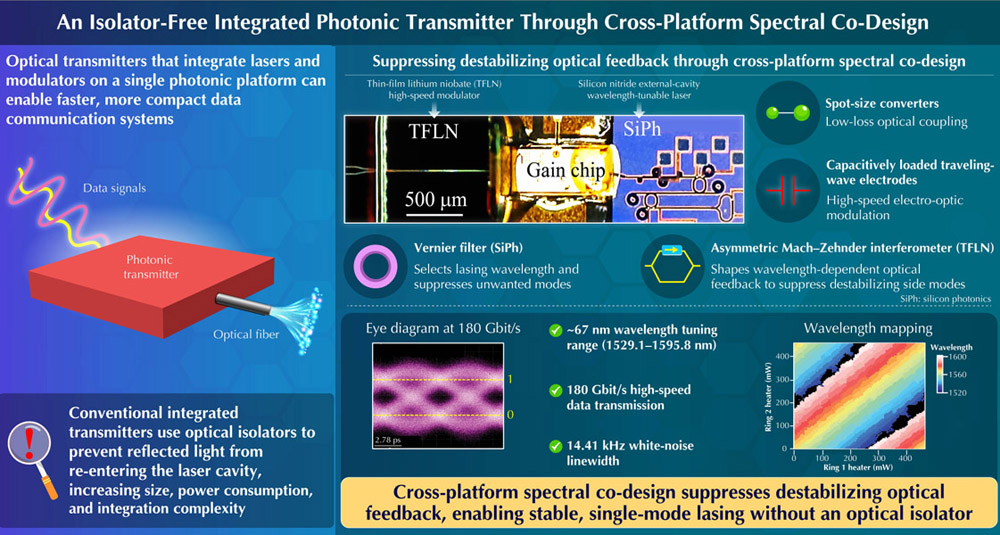
The transmitter combines silicon nitride ring resonators, which provide wavelength-selective filtering, with a thin-film lithium niobate modulator capable of high-speed data encoding. Coordinating their optical responses enables stable laser operation without an optical isolator, with data transmission speeds of up to 180 Gbit/s. Image credit: Professor Tomohiro Kita from Waseda University, Japan.
Growing demand for faster data exchange between data centers calls for compact, high-speed optical transmitters. Researchers from Waseda University, in Japan, have developed an integrated optical transmitter that mitigates the destabilizing effects of unwanted optical feedback, allowing stable laser operation without an optical isolator. The device operates across a wavelength range of approximately 67 nm and demonstrates data transmission at 180 Gbit/s, offering a promising approach to compact, high-capacity optical communication systems.
The work is described in the Journal of Lightwave Technology.
The growing use of generative artificial intelligence (AI) and cloud services is increasing data exchange between data centers, creating a need for faster, more energy-efficient, compact optical transmitters. One promising approach is to integrate silicon photonics-based tunable lasers, which generate light at different wavelengths, with thin-film lithium niobate (TFLN) modulators, which encode data onto light at high speeds.
However, integrating lasers and modulators built on different platforms can introduce unwanted optical reflections from the modulator back into the laser. These reflections can destabilize the laser and disrupt data transmission.
Research and team
Conventional systems use optical isolators to block backward-travelling light and protect the laser from unwanted reflections. Researchers, led by Professor Tomohiro Kita of the Department of Applied Physics at Waseda University in Japan, developed an integrated transmitter that controls wavelength-dependent optical feedback through cross-platform spectral co-design, allowing the laser to operate stably without an optical isolator.
The research team also included Shotaro Hirata, Shingo Takano, Yu Kataoka, and Ryo Shimizu, researchers at Sumitomo Osaka Cement Co., Ltd., Japan, and Dr. Yuya Yamaguchi of Japan’s National Institute of Information and Communications Technology (NICT).
“This architecture provides a promising pathway toward compact, isolator-free optical transmitters for next-generation photonic integrated circuits and high-speed optical communication systems,” said Kita.
The transmitter combines an external-cavity wavelength-tunable laser, formed by a semiconductor gain chip and a silicon photonics circuit containing two silicon nitride ring resonators, with a TFLN modulator incorporating an asymmetric Mach–Zehnder interferometer (AMZI). The two ring resonators form a Vernier filter that selects the lasing wavelength, while the TFLN modulator encodes high-speed data onto the optical signal.
The AMZI has a wavelength-dependent transmission response. By co-designing this response with that of the SiN Vernier filter, the researchers shape the wavelength-dependent optical feedback returning toward the laser and mitigate its destabilizing effects. This cross-platform spectral co-design enables stable single-mode laser operation without an optical isolator.
The transmitter can operate across a broad range of wavelengths, approximately 67 nm, while maintaining a stable laser output even without active temperature control. The researchers also demonstrated data transmission at 180 Gbit/s, the highest data rate investigated in the present experiment, with test results showing that the optical signals remained distinguishable at these high speeds.
By eliminating the need for an optical isolator, the design could simplify the optical transmitter’s design and potentially reduce its footprint, making it easier to integrate different photonic technologies into compact devices. Such a design could be particularly useful for high-capacity optical connections between data centers, including AI data centers, which need to transfer large amounts of data quickly.
“The technology is particularly relevant to high-capacity optical interconnects between data centers, including AI data centers. Its broad wavelength tunability makes it suitable for wavelength-division multiplexing, in which multiple data channels at different wavelengths are transmitted through a single optical fiber,” said Kita.
 Eulitha ramps output of its lithography systems for AI data center lasers
In related news, Eulitha AG, a provider of high-throughput optical lithography solutions, based in Würenlos, Switzerland, has announced deliveries of multiple automated tools to foundries for the production of indium phosphide (InP) DFB lasers to be used in AI data centers. The company has also reported that it currently has an order backlog that will fully occupy its production capacity until the middle of 2028.
The DUV photolithography tools are based on the proprietary DTL technology developed and commercialized by Eulitha, enabling the printing of high-resolution gratings required in DFB lasers.
DFB lasers are at the center of optical communication solutions that are required to move data at high speeds between AI chips and memory or other processors, as well as over longer distances between racks and data centers, says the firm. The use of optical communication and co-packaged optics (CPO) promises to significantly reduce energy consumption while dramatically increasing the speed of AI systems and data centers.
These lasers require printing high-fidelity, high-resolution gratings for precise wavelength selection. Eulitha has been working with leading device manufacturers to provide the lithography tools that meet the rigorous quality and volume requirements of the booming AI market.
Harun Solak, CEO of Eulitha, said, “Multiple DFB manufacturers have been using our tools for production for a number of years, but the volumes we have seen since 2025 represent explosive growth due to the expansion of data centers. Our technology is matched to address this patterning challenge with its high precision, resolution, and throughput. Our customers, for whom the alternative was to purchase tens of e-beam tools, are able to save significant costs by choosing our photolithography technology.”
Eulitha is currently doubling its production capacity at its location near Zurich, Switzerland, to meet the growing demand. The new production capability is scheduled to come online during the first quarter of 2027. The expansion will allow Eulitha to meet the growing demand for affordable, high-resolution patterning tools not only in optical communications for data centers but also in other areas such as light guidance for AR/VR/XR devices.
Laser weapons and battery welding aid IPG Photonics sales growth
November 04 2026
Rockefeller University microscope points to deeper brain imaging
November 04 2026


Europe-Japan group to industrialize flexible perovskite solar cells
November 03 2026

Marvell set to acquire Lumentum in $115BN all-stock deal
November 03 2026